| Table of Contents | ||
|---|---|---|
|
Quick Start Guide
- Enable the tool in Coral.
- Determine the correct objective(s) (10X, 25X, and 63X available) for your application.
- Select the objective in the microscope control console near the keyboard.
- Ensure the Process light on the tool (green) is not lit. If it is currently lit, ensure that the Holder Exchange dialog is open. If not, click Exchange Holder.
- Press the Open button, it should flash and the lid can now be opened.
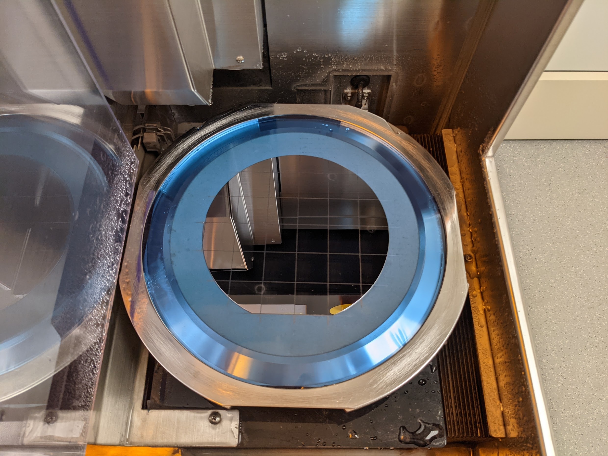
- Open lid and sample holder lid.
- Remove black cap from center-most microscope position, install the objective
- Objective should be inserted only until rotation stops. Do not overtighten.
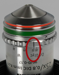
- For the 25X objective, ensure the correct Adjustment Ring setting is selected. For most cases, Glyc with the 3 longest bars is used.
- Install resin stop on the objective.
- For 10 and 25X, a silicone stop is used. For the 63X, a fiber ring is used.
- Select an appropriate sample holder and place on the white and black support with the Resist side facing up.
- Place your substrate in the holder and tape down with at least two strips of tape from the dispenser.
- Place a drop of resin on the substrate.
- For 63X oil-based printing, please be sure to place the oil on the proper orientation - the oil should be in contact with the lens, not the resin
- Ensure the sample holder lid in the printer is placed in the partially opened position, supported by the latch.
- Bring sample holder to printer. Immediately before inserting, flip sample holder upside-down and insert in the printer.
- For all resin-based prints, the resin side of your substrate should be facing the objective.
- For oil-based printing, the oil side should be facing the objective
- Close sample holder lid and secure down with both clamps.
- Ensure all lens holders, tools, etc. are clear of the tool and close the main lid.
- Select the correct sample holder and sample position in the Exchange Holder dialog box.
- For standard prints, click Approach Sample. For manual interface finding, please see the information provided in Manual Interface Finding.
- Click Load Job and select your *_job.gwl file.
- Click Start Job.
- When printing has finished, click Exchange Holder. Leave this dialog box up for the next user.
- Partially open sample holder lid and remove print, inverting it so that it is resin-side up.
- Open sample holder lid and remove the objective; you may leave the resin stop on if there is resin on it during this process, otherwise you may remove the resin stop first.
- Clean objective as outlined in objective cleaning
- Log out from tool
- Develop your samples as outlined in the sample development section
Introduction
Direct laser lithography or direct laser writing using two-photon femtosecond near-IR laser for additive manufacturing using conventional resin sensitive to two-photon absorption resulting in two-photon polymerization to create volumetric prints from CAD models.
Exposure System
The NanoScribe GT2 Laser Lithography System is an ultramodern two-photon polymerization volumetric maskless printer. It is one of our newest acquisitions here at the Cornell NanoScale Facility (CNF). The tool was purchased in late 2019 and delivered and installed during the second week of January 2020. This was accomplished with the help of a committee of faculty and researchers, and a grant from the NSF. The NanoScribe GT2 can create three-dimensional nanostructures using a NIR femtosecond laser via direct-write onto a photosensitive resin, which is subjected to a non-linear two-photon absorption process. This process involves cross-linking the resin via UV absorption. The laser sets a focal light cone where a concentration of the light intensity defines the exposure focal spot volume or a “3D Pixel.” Using this technique, a CAD design can be broken into an X-Y-Z coordinate system to define the structure pixel by pixel and layer by layer. The exposure side of the system sits in a fine-tuned vibration isolation table and a high-speed ultra-precise piezoelectric stage for movement in X-Y-Z and uses a galvanic mirror defection system for focusing and beam rasterization. Models for printing can be designed using the stand-alone software DeScribe—which comes with the tool—or with any CAD software capable of outputting file formats DXF or STL. The DeScribe software can import these formats.
3D Print Technology & Direct Write
Laser-based direct writing has been around for a few years especially in the semiconductor industry known as maskless lithography (MPL). Typically, the two-dimensional CAD design is transferred onto the substrate that is pre-coated with a photosensitive resin via reduction laser projection. The projected pattern was reduced given the tool's numerical aperture and scan across the surface of the substrate using either a raster or vector format. These techniques are the same ones utilized in 3D direct-write. The only difference is that now you are working with a thickness degree of freedom that can be scanned across the Z-axis. The NanoScribe GT2 has a Piezo Nanopositioning stage and a high-speed galvo scanner. In the case of two-photon lithography, the light source is a pulsed femtosecond fiber laser with the center wavelength being around 780 nm.
Hardware Overview
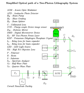
Diagram of a simplified optical path of a Two-Photon Lithography System.
Utilized Objectives [NA: 10x, 25x, 63x]
The 25X has an adjustment ring for printing with different liquids. For most cases, the Glyc setting with the three longest bars is used, as shown below:
Two-photon Light Source
- Hight Performance NIR femtosecond laser [FemtoFiber Pro]
Training
Cornell NanoScale's Training Workflow
- Send the tool manager a request for online access to NanoScribe’s NanoGuide Webpage.
- Meet with the tool manager to discuss your project.
- Complete the CULearn training for the tool.
CULearn Training links:
- RSRCH - CNF - NanoScribe GT2 (NetID Link)
- RSRCH - CNF - NanoScribe GT2 (GuestID Link)
- Once you completed the CULearn video and quiz, email the tool manager to schedule a hands-on training session.
- Users are required and responsible for reviewing the services and procedures provided by NanoScribe on the following:
- You will need to log in to NanoGuide to view these materials.
- Model Creation (CAD)and Import
- Printing
- Print with Solution Sets
- Print Applications
- Print Strategies
- Programming Structures
- Post Print Processes
- Further REading
- You will need to log in to NanoGuide to view these materials.
- Check your STL model for common mesh errors. You can use CAD software capable of mesh verification such as Autodesk Meshmixer or MeshLab
- Once your file has been checked for mesh errors, run it through DeScribe to do the conversion. Be sure to select the desired solution set (SF, MF, or LF) for your process.
- Once the CULearn
NanoScribe's Subsystems
Electronics Cabinet
Optics Cabinet [contains the laser, optics, and Galvo]
Emergency Off (EMO) switch
Printing Cabinet [Microscope, Piezo, and Stage]
Power Supply 232
System Controller
System Computer
Laser System Controller
Galvo Stage Power Supply
Monitor, Keyboard, and Mouse
Manual Microscope Controller
Joystick
CAD & Software
CAD Model
Since NanoScribe only handles the fracturing and slicing of the imported CAD design utilizing its own proprietary General Writing Language (GWL) complex models need to be designed and verified outside of the system and when ready exported as a Standard Triangle Language or Standard Tessellation Language (STL). STLs describe the raw unstructured triangular surface geometry of three-dimensional using normalized units and vertices objects without any color or texture attributes. STLs can be written in both ASCII and binary.
3D CAD Software Available at the CNF
Note: Software usage is limited and or restricted depending on the type of license the CNF currently is under contract.
...
You may opt to use the CNF 3D GPU Conversion Computer which has a number of software tools above as well as DeScribe available. Compile time on DeScribe is typically faster on this system than a standard Windows desktop PC by 2-3 times for complex 3D object. Instructions for its use are available here.
STL Conversion From GDSII Files
GDSII files are common for traditional photolithography processes and it is possible to convert them to a 3D model suitable for use with the DeScribe slicer. Three primary applications are used in this process:
...
Installation is easiest on a Linux distribution. General installation instructions are available on the gds3xtrude link.
DeScribe
- Options for running DeScribe Software
- The most current version is v2.7 as of 12/7/22
- It is highly recommended that you use the most current version of DeScribe to have access to the latest recipes and print modes.
- In v 2.7, most recipes are included in DeScribe and do not need to be downloaded separately
- Users can download their copy here (requires software license and Nanoguide access)
Recipes: DeScribe Tabulated Solution Set based Parameters:
| Solution Set | Objective | Resin | Substrate | Sample Holder | Slicing | Hatching | Dev/Rinse |
|---|---|---|---|---|---|---|---|
| SF | 63x | IP-L / IP-DIP | Fused Silica / Borosilicate Substrates | DILL / DiLL Oil | 0.3 um | 0.2 um | 12 min |
| MF | 25x | IP-S | ITO-Coated | DiLL | 1 um | 0.5 um | 20 min |
| LF | 10x | IP-Q | Silicon | DiLL | 5 um | 1 um | 20 min |
Printing Modes
The Nanoscribe uses solution sets which are paired to an objective in order to slice a CAD model. In general, each objective has a Solid, Shell and Scaffold, and Swift printing mode.
| Mode | Use Case |
|---|---|
| Solid | Slowest printing method, generates parts which do not require post-process UV curing generally. High resolution printing. Used for delicate or intricate parts where strength is a priority or long development times are required. |
| Shell and Scaffold | Faster than solid, speed dependent on part complexity and infill percentage. Parts have a high resolution shell with coarse infill to balance speed and high resolution. Will require UV cure. Used for intricate parts where development times are short (<<1hr). |
| Swift | Fastest printing method, prints coarsely in a layer-wise fashion in half the time of most shell and scaffold prints. Parts usually do not require UV cure. Balanced Swift is higher resolution than Swift, but longer print times. Used for bases or support structures where dimensional accuracy is not critical. |
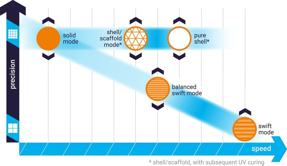
Comparison of printing solutions by part resolution and print speed. Image from Nanoguide
NanoWrite
Sequence Of Operations

General Printing: Operational Workflow (SOP) as stated in the NanoGuide
The basic standard operation procedure (SOP) is summarized below. The titles link to pages with more detailed information.
The paragraph headers of this page link to important safety measures. Carefully read through each article to avoid harm to the operator and damage to hardware components. Additionally read through printing considerations, which provides general information for a successful print along with best practice advice.
Check the status of the printer
- Make sure the printer components are switched on. If the laser was switched off wait for 30 min before starting a print job to ensure a stable laser output.
Import a CAD model file
- Drag and drop an STL file (CAD model file) into DeScribe to start the import wizard.
- Center the model and adjust the orientation as well as size. Ensure that it fits within the substrate dimensions and consider the working distance of the objective for the desired print set.
- Choose a recipe matching the desired print set and follow the steps given in the import wizard.
- Save the GWL print job file.
- Preview the print job (shortcut: F5 key).
- Alternatively, the print job can be programmed manually.
- If the import was performed on a personal computer, copy all GWL files and the subfolder "..._files" to the control computer.
Prepare a sample and change the objective
- Prepare the required materials for the intended print set and print job.
- Fix the substrate to the sample holder and apply resin.
- Check that the resin is free from bubbles.
- Select an objective and inspect it for cleanliness. Clean it if necessary.
- Use a clean and dry felt ring or resin stop with all objectives except for air objectives.
- Wash felt rings with isopropanol before the first use to remove loose fibers.
- Mount objective in the correct position. Use the touch screen to check/select the position if necessary.
Start NanoWrite and insert sample holder
- Start NanoWrite.
- Wait for the stage calibration warning message.
- Ensure sure the stage will not be impeded by obstacles.
- Ensure the microscope objective is at the lower z-drive limit.
- When it is safe to do so, confirm the warning message by clicking Calibrate.
- Wait for the NanoWrite initialization to finish.
- When the Exchange Holder dialog appears, carefully insert the sample holder.
- Select the correct sample holder and sample position from the dialog box.
- Confirm the selection by clicking OK.
- Switch on an illumination. Choose reflection illumination for non-transparent substrates.
- Start AxioVision software and position it next to NanoWrite to view the print process in real-time.
Perform a sample approach
- Ensure that the selected sample position is correct. If it is not, double click the respective position on the sample holder icon in NanoWrite.
- Click Approach sample to move the objective towards the interface. The interface will be automatically found and the working distance set such that the interface is in focus. The result of the interface approach is displayed in the NanoWrite message log window.
- Adjust the brightness and contrast in the AxioVision software.
- After each subsequent movement of the stage, the interface position must be verified. Either click Find Interface to autofocus the interface again, or issue FindInterfaceAt commands in the GWL code of the print job. Imported models utilizing block splitting and stitching have the commands included automatically.
Load a print job
- Click Load Job and choose a print job (name_job.gwl file).
- Wait for loading to finish (indicated by name_job.gwl loaded in the message log window).
- If compilation takes a long time, use DeScribe to perform this step (debug -> compile, or shortcut: F5)
Print your structure
- For high-precision applications allow ~30 min for the resin and holder to reach thermal equilibrium.
- Click Start Job.
- Wait until the print job is finished or press Abort to immediately halt the job.
Unload the sample
- Click Exchange Holder.
- Wait for the Exchange Holder dialog to pop up.
- Carefully remove the sample holder.
- Confirm the dialog by clicking OK.
Develop the sample
- Carefully remove the substrate from the sample holder.
- Place the substrate in a developer bath (PGMEA for most resins, methanol for GP-Silica) to wash away excess liquid 2PP resin.
- Leave substrate in developer at least 15 minutes, high aspect ratio structures require additional development time.
- Wash away the developer with IPA.
- Transfer to IPA for at least 15 minutes.
- Cure remaining liquid 2PP resin if a shell and scaffold structure was printed.
Clean the objective lens
NEVER USE ACETONE WHEN CLEANING THE OBJECTIVES
- The objective lenses must be thoroughly cleaned after each user has finished using the tool. Multiple prints may be conducted during the same user session without the need to clean the objective, assuming the same 2PP resin will be used for each print.
- In most cases, IPA alone is appropriate for lens cleaning.
- Specific lenses have different cleaning requirements, as do different resins and immersion oils.
- If you are unsure of the proper cleaning procedure for your use case, please contact the staff before printing.
10X Objective
- Remove the objective and screw it into its holder
- Carefully wipe the metal portion of the objective with a lab wipe or swab, taking care not to touch the glass.
- Cover the lens with the clear top cover and move the lens to the development room.
- Place the lens on clean wipes where you will be cleaning - do no assume wipes left in the hood are clean.
- Carefully fold a wipe to about 1 to 1.5" wide and wrap around the body of the objective. Take note of the location of the vent hole by placing your thumb directly over it.
- Invert the lens over the waste container and funnel.
- Gently flow IPA over the objective using a wash bottle - be careful to dispense the IPA slowly and keep the tip of the bottle away from the nosepiece.
- With the lens still inverted, use the N2 blowgun and dry off the IPA with a low pressure stream of dry nitrogen
- Return the lens to an upright position and using a wipe or swab remove any resin which has flown onto the metal body of the nosepiece
- Repeat, typically 2-3 additional times, using IPA sparingly.
- Note, for use with GP-Silica, alternate cleaning methods must be used, as outlined in the section on GP-Silica
25X Objective
- Remove the objective and screw it into its holder
- Carefully wipe the metal portion of the objective with a lab wipe or swab, taking care not to touch the glass.
- Check the objective body, and in particular, the adjustment ring for any residual resin and clean this with a lab wipe dampened with IPA.
- Cover the lens with the clear top cover and move the lens to the development room.
- Place the lens on clean wipes where you will be cleaning - do no assume wipes left in the hood are clean.
- Carefully fold a wipe to about 1 to 1.5" wide and wrap around the body of the objective.
- Follow steps 6-10 as above, being careful to prevent any IPA from coming into contact with the rubber gaskets and the adjustment ring in particular.
63X Objective
Follow cleaning for the 10X objective, omitting the need to cover a vent hole in step 5.
...
Failure to properly maintain the objectives can and will result in significant tool downtime.
Leaving the printer
- Clean the workspace with a wipe and 70% IPA spray to ensure there is no residual resin on the desk or the printer.
- Ensure the sample holders are clean and free of resin and wipe with 70% IPA is any residue is left on them.
- Close NanoWrite. This makes sure that used print commands are set to the default values for the next user.
- Only switch off the laser and other printer components if the printer is not in use for a longer period of time.
Material Specifications for standard printing at CNF
Substrates Specifications
| @ 780 nm | Fused Silica Substrates | ITO-Coated Substrates | Silicon Substrates | Borosilicate Substrates | Microscope Slides |
|---|---|---|---|---|---|
| Material | Fused Silica | Soda Lime w/ ITO | Si Substrates | Borosilicate Sub | Microscope Slides |
| Sample Holder | DiLL | DiLL | DiLL | 10 × Ø 30 mm | DiLL |
| Refractive index | 1.454 | 1.624 [ITO] 1.518 [soda lime] | 3.710 | 1.517 | 1.518 |
| Dimension | [25, 25, 0.7] mm | [25, 25, 0.7] mm | [25, 25, 0.725] mm | 30 mm Ø, 170 µm | [22, 75, 1] mm |
| Thickness variation | ± 25 µm | ± 60 µm | ± 25 µm | ± 10 µm | ± 100 µm |
| Surface finish | DSP | DSP | Polished | DSP | DSP |
| Density | 2.2 g/cm3 | 2.5 g/cm3 | 2.3290 g/cm3 | ||
| Mohs hardness | 5.3-6.5 | 5-6 | 9-10 | ||
| Melting point | 1400°C | 1000°C | 3265°C | ||
| Thermal expansion coefficient | 0.54x10⁻⁶ K-1 | 0.937 W/m·K | 2.6 µm/(m·K) | ||
| Heat conductivity | 1.38 W/(m·K) | 0.937 W/(m·K) | 149 W/(m·K) | ||
| Compatible w/ Solution Set | 3D SF | 3D MF (3D SF, 2D ML) | 3D LF (3D MF, 3D SF, 2D ML) | 3D SF Oil | 3D SF |
| Compatible w/ 2PP resin | IP-DIP | IP-S | IP-Q (IP-S, IP-Dip, AZ resin) | IP-L 780 or IP-G 780 | None, unless coated |
| Compatible w/ Objective | 63X | 20x, 25x , 63x | 10x, (20x, 25x, 63x) | 63x | 63x |
| Combination & Ref index | -0.058 @ 20°C IP-Dip / -0.025 @ 20°C IP-S | -0.145 @ 20°C | |||
| Contrast | |||||
| Cleaning & Prep | O2-plasma & silanization | O2-plasma & silanization | RC1 |
...
| ITO | Value |
|---|---|
| Film Thickness | 18 nm ± 5 nm |
| Film Surface Resistance | 100 - 300 Ω |
| Film Transmittance | ≥89% |
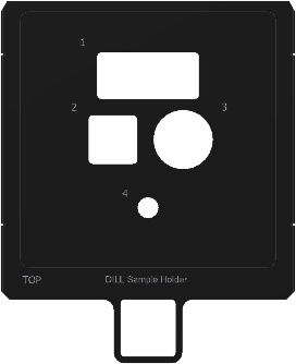
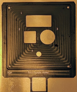
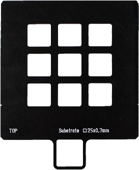
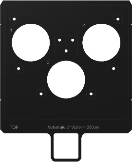
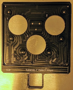
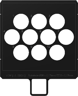
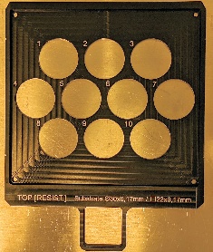
Sample Holders available at the CNF
| Sample Holder | Substrate Type | Substrate Thickness | Holder Image | CAD Files | ||||||||
|---|---|---|---|---|---|---|---|---|---|---|---|---|
DiLL |
|
|
| |||||||||
| Fused Silica Substrate, ITO-Coated substrate, Silicon Substrate: 25 x 25 mm² | 0.70 mm, 0.70 mm, 0.725 mm | 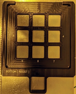 | *Note: some dimensions are approximated | ||||||||
2" Wafer | Ø 2 inch Wafer | 0.35 – 0.55 mm |
| |||||||||
10 × Ø 30 mm | Ø 30 mm | 0.17 mm |
|
Resins Available at the CNF
|
|
|---|
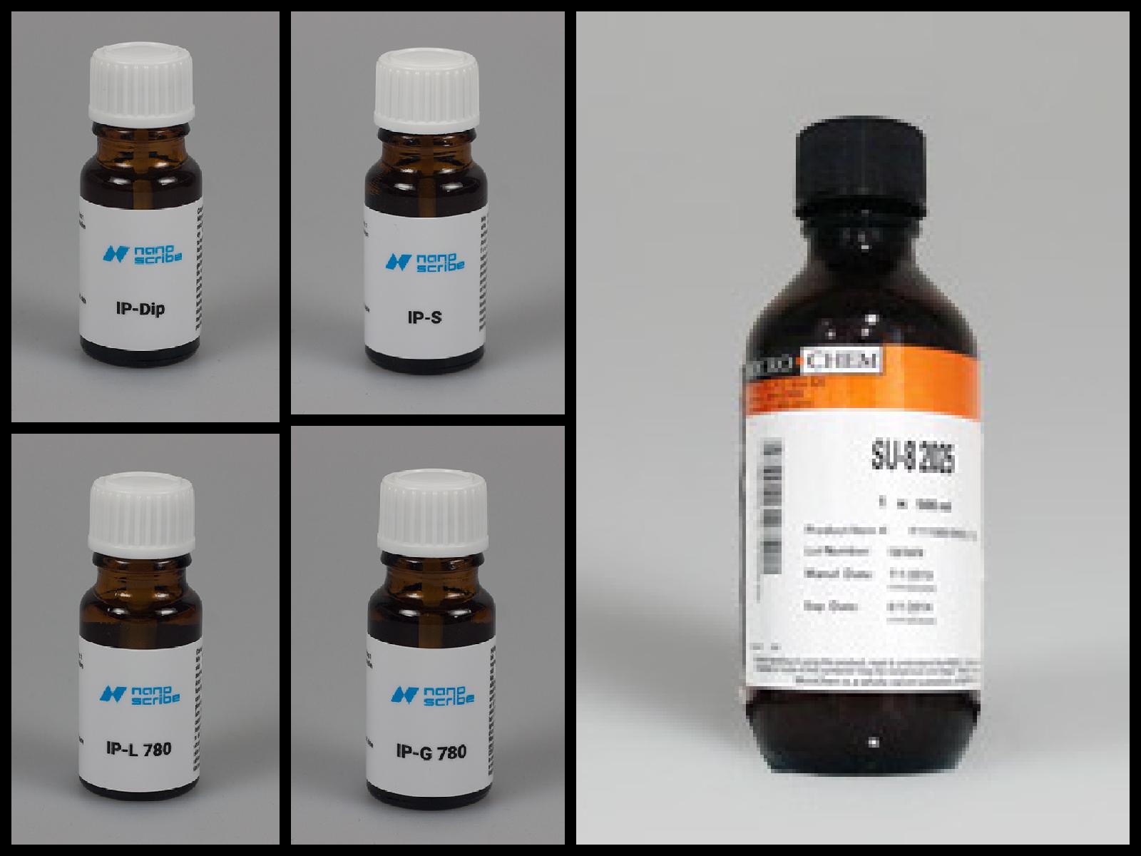
GP-Silica Resin
A new resin will soon be available for use. GP-Silica contains silica particles which can be sintered into solid fused silica parts. Using the LF solution set, users can develop robust parts with mechanical and optical properties very similar to bulk fused silica.
...
- Maximum part printing time of 15 hours - exceeding this time may cause severe lens damage, as the resin will slowly cure and solidify over time.
- Parts must be developed in methanol and should develop horizontally to prevent premature part-substrate separation
- After development, parts must be sintered to come to full strength. Currently, CCMR's controlled atmosphere furnaces are recommended for thermal processing. Sintering curves are available on Nanoguide.
Developer
- PGMEA (CAS NO. 108-65-6) (For IP-Dip, IP-S, IP-Q, IP-L, SU-8)
- Methanol (CAS No. 67-56-1) (For GP-Silica only)
- Isopropanol (CAS No. 67-63-0) (For secondary wash, all resins)
Metrology & Post Processing
Model UV Curing
- Parts, particularly shell and scaffold components, may require a UV cure after development.
- Shell and scaffold parts contain uncured resin within solid walls. Failure to UV cure will result in weak parts and may leak resin.
- The resin's highest sensitivity is to 405 nm UV, however broad spectrum UV curing stations may also work.
- NOTE: The resin may burn or become distorted with UV power densities above 7 W/m2
- Typical maximum cure depth is 2.5 mm
- Recommended exposure time is 1-15 minutes, dependent on part geometry
- Alternately, parts may be heat cured. IP-S cures in 5 minutes at 190°C and 17 h at 140°C. Care must be taken to slowly heat samples; thermal shock may break your part off the substrate prematurely. IP-DIP and IP-L cannot be heat cured.
UV Cure Station
A 405 nm UV cure station is available in Room 121 in the cleanroom.
Technical Specifications:
- Fourteen 405 nm LED in two arrays (2x7)
- Maximum 40W total LED power
- Fluence: 21 mW/cm2
- Solar powered rotating stand
- Maximum running time of 40 minutes. Exceeding this may cause damage to the equipment.
- Typical exposure time of 0.5 - 10 minutes.*
...
Note – the LED lighting is diffuse, making characterization of the exact energy density your sample will receive difficult to estimate, as sample location and height can have a significant impact on energy received. Overexposure of samples to 405 nm light may result in yellowing of the samples and embrittlement of the resin.
Use
Can be used for curing 405 nm wavelength resists/resins, particularly parts printed on the Nanoscribe Photonic Professional GT2. Users should only place clean, dry parts in the cure station. Users are responsible for cleanup after use, including wiping the stand. This cure station will run for a user-selected time and automatically shut off after the time has elapsed. Time is entered in 30 second increments up to 40 minutes. Generally, curing times will be well under 10 minutes. Running for 40 minutes or longer may result in overheating of the machine. Samples are visible through a yellow filter in the front of the cure station – you may notice intense fluorescence of your samples while the curing is ongoing.
Safety
This curing system uses near-UV 405 nm wavelength light, which is not inherently harmful to vision or cells. The lighting system is, however, very bright posing a risk of vision damage if the system is operated without being properly closed. Filtered goggles are available and encouraged for users. Additionally, the bright light may cause unwanted curing of other samples when open. As such, the station should only be run when in the properly seated closed position and only opened when the LED array is off.
Model Removal
After printing and development, parts that are still on the substrate may need to be removed if they have no detached already. For robust parts on substrates that have poor adhesion, particularly silicon wafers, parts may be detached through simple mechanical means. However for more delicate parts or substrates with superior adhesion, a few methods can be used to remove parts:
...
In some cases, sonication in IPA may work to dislodge a part from its substrate, using short durations (<1 min) and checking your part often.
Silicon Wafer Substrate Production
Standard Type P silicon wafers can be cut to produce 25mm square substrates for use with the 10X and other processes using the CNF DISCO Dicing Saw. Users must provider their own wafer for slicing; for best results, wafers should be 700µm thick +/-25µm. After receiving training on this tool, a program has been saved that is available to dice 6" wafers for use in the Nanoscribe. When using the DISCO Dicing Saw, open the USER directory and select the Nanoscribe6in profile. Please note: this profile is currently set for a 675µm thick wafer; you MUST adjust this parameter for thicker or thinner wafers.
...
Once you have completed the alignment process (typically aligning only along the flat edge of the wafer is adequate), a total of at least 18 substrates will be produced. Take care to ensure that substrates are free of debris from cutting before using in the NanoScribe. Additional cleaning of substrates via sonication with consecutive baths acetone, IPA, and DI water is recommended.
Advanced Printing Procedures
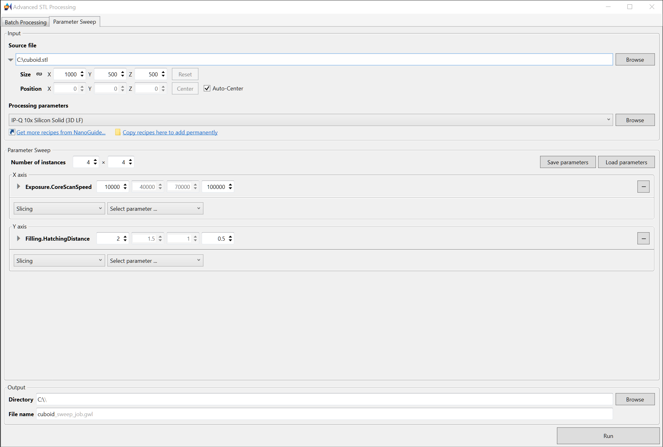
Parameter Sweeps
While the default DeScribe settings work in many cases, high precision parts may require careful tailoring of the printing parameters, such as laser scan speed, laser power, hatching distance, among others. The quickest way to test a variety of these parameters is with the Advanced STL Processing tool in DeScribe. Using a test STL, usually a small part or feature, one can generate a 1D or 2D array of parts with parameters varied between a start and end point. The image below illustrates a 4x4 array which varies scan speed and hatching distance, which impacts effective laser dose and can highlight issues due to proximity effect:
File Generation and Hierarchy
Advanced printing procedures often require modification to the basic files generated by the DeScribe slicer. In addition to offering much greater control over your print, a user can stitch together multiple jobs into a single part with differing print modes, or even objectives. Many of the most useful commands are highlighted in the sections below. A full reference list is available on Nanoguide and in the DeScribe editor under Window → Command Reference.
...
sample_files - This folder holds the GWLB, or binary GWL files which are ultimately read by the printer and dictate the laser paths and stage movements. These files are binary and not easily readable or editable.
Multi-DiLL Printing
Multiple samples can be printed sequentially without the need to open the printer and switch substrates. This is useful for jobs where a large number of samples are needed, particularly if print times are short. The procedure for setting up a Multi-DiLL print will reference this build folder which is available for download: Sample01_02_03.zip The builds are based on these simple STLs: sampleSTLs.zip.
...
- Load the *job.gwl file in your top folder in NanoWrite, in the case of the example load 1_2_3_job.gwl
- Start print job, the total print time scales linearly with the number of samples in the job
Manual Interface Finding
WARNING: MANUAL INTERFACE FINDING MAY RESULT IN A COLLISION BETWEEN THE SUBSTRATE AND LENS IF DONE IMPROPERLY. IF YOU HAVE CONCERNS, PLEASE CONTACT A STAFF MEMBER BEFORE ATTEMPTING.
...
*Note - the Z values in this video are not necessarily reflective of other prints and should not be used as a reference.
Printing on Porous Substrates
For substrates with holes or other features, it is necessary to manually align the microscope. First, users should follow the Manual Interface Finding procedure. This can be done on any location on your substrate, however an area away from your desired print area is suggested. Once an interface has been determined, manual alignment can begin.
...
These substrates were printed via an SLA process at 50um layer height and subsequently polished to a 3um finish.
Multi-Part Printing
The Nanoscribe is capable of printing multiple parts in a single job, assuming they use the same objective.* In general, each individual part is sliced with its own parameters and then a master job.gwl file calls these individual parts.
...
*Multi-objective printing is also possible, but not covered in this example.
Marker Alignment
Printing on wafers prepared by other systems or prints that require multiple objectives may require special alignment procedures to ensure the print occurs in the exact orientation desired. A detailed description of the exact alignment procedure is available on Nanoguide. To aid with this, three job files have been prepared to aid in aligning the 10X, 25X, and 63X objectives. All files by default print a single voxel width X for orientation purposes using the Write command. An example of this is below:
...
Applications
- Microfluidics
- Micromechanics
- Biomedical Engineering
- Micro-electro-mechanical systems
- Mechanical metamaterials
- Micro-optics
- Photonic metamaterials and Plasmonics
Study highlights promise of 3D printing for electrochemical reactors [04/2021]
Nano-sized McGraw Tower features 161 steps, chimes [05/2021]
Biologically inspired micro-robotic swimmers remotely controlled by ultrasound waves [09/2021]
- Building the Nano-3D McGraw Clock Tower [12/2021]
Other Files
Users may wish to store their new and used 25mm square substrates. A set of STL files is provided for users to download and 3D print; each holder can fit 20 substrates.
...
It is recommended that these be printed with an SLA or similar process, as tolerances are tighter than allowable by FDM printing.
Other Sites in the NNCI Network with a NanoScribe
Stanford University: Stanford Nanofabrication Facility
Harvard University: Center for Nanoscale Systems
- Georgia Tech: Institute for Electronics and Nanotechnology Micro/Nano Fabrication Facility
- University of Kentucky: Center for Nanoscale Science and Engineering
- University of Pennsylvania: SINGH Center for Nanotechnology
Power UP and Power DOWN Procedures [STAFF ONLY]
Power UP Procedure
Warning!
"Disregard of the guidelines concerning power-up of the Photonic Professional GT2 may cause damage to the system!"
...
Turn the mains power switch to position 1.
Wait some seconds until the reset and open buttons blink in alternation and the attention indicator is lit up.
Press the reset button, the attention indicator switches off.
Switch on the Photonic Professional GT2 Controller by activating the key switch.
Switch on the Control PC: Let it boot completely before proceeding, wait until the long on-screen shows up.
Switch on the laser controller by activating the key switch. The button
start/stopdoes not have to be pushed (the backlight of the button should be off). The laser emission is controlled via the Photonic Professional GT2 control software NanoWrite.Switch on the GT power supply.
Switch on the z-drive power supply.
Switch on the computer monitor.
Press the open button in order to release the safety lock and to open the printing cabinet. As long as the safety lock is released the open button is blinking white.
Note: The laser gives acoustic feedback, as soon as its start-up is finished. This can take up to 30 s. After that, the control software NanoWrite may be launched. Make sure that the laser is operational when starting NanoWrite. The laser emission is switched on automatically when NanoWrite starts. The status of laser emission is indicated by the backlight of the button
start/stopon the front panel of the laser controller. If the light is activated, the emission is on. You can manually switch on/off the emission by pressing this button. A power calibration of the laser is performed automatically before the first print starts or when NanoWrite receives the first script command.
Power Down Procedure
Warning!
"Disregard of the guidelines concerning power-up of the Photonic Professional GT2 may cause damage to the system!"
...