ASML – "Super Tapper"
Background
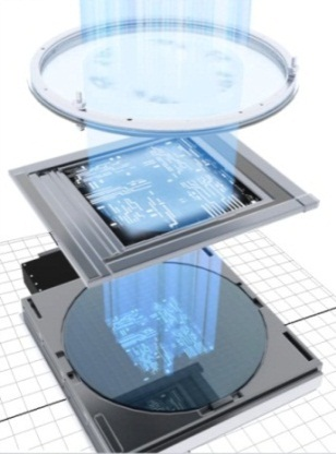
Whether you are reading this on a computer, on a smart phone, on a tablet, or on any other device, you are using ASML's lithography products right now. In lithography, an image on a reticle is projected onto a wafer to etch the design into the wafer. Figure 1 shows a simplified version of some of the key components in the process. The bottom section shows the round wafer in a square carrier, while the middle section shows the rectangular reticle. The top circular section is part of the optical system.
|
Figure 1 – Simplified Lithography Process |
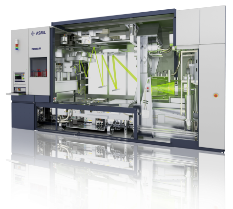
Improvement in the lithographic process is so important because as lithography improves, so does the speed and capability of the microchips that are created from the process. Following "Moore's Law", advances in lithography systems, such as the one shown in Figure 2, have allowed chip manufacturers to continue to shrink feature sizes, with the current state of the art possessing the ability to manufacture feature sizes in the range of 22 nanometers, or about the size of 100 silicon atoms.
|
Figure 2: Lithography System |
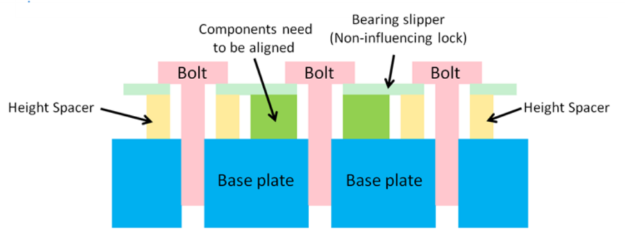
With feature sizes in that range, tolerance budgets are pressed to the atomic level. All components and processes contributing to the precision of the equipment must be optimized. For example, placement of components must be precise, requiring state of the art mechatronics and metrology equipment. Many components are located precisely enough with respect to the housing or baseplate to which they interface by carefully budgeting and specifying tight machining tolerances in our drawings. However, for some other components, extremely tight positioning requirements, combined with tolerance stack-up exceed what can be achieved by precision machining. In those situations we have no other choice than making the assemblies adjustable with respect to the housing. A tried and true design approach for achieving high precision and stability with an adjustable interface is the "bearing slipper", which is discussed below.
As an example, when adjusting precision mechanisms that have a bearing slipper locking, shown in cross section in Figure 3, often we need them to move by known small increments. "Tapping" provides a convenient means of making small adjustments with minimal tooling. However, due to the non-linear nature of friction (stick/slip), the increment of motion is not easily controllable, and external means (typically a gauge) are needed to measure how much movement has occurred. Precision gauges are readily available; however having to provide mounting interfaces in the housing substantially complicates the design and creates volume conflicts. In addition, manual tapping is essentially a trial and error process guided by "feel", and not everyone has the skill to converge within the specified precision in a reasonably short time.
|
Figure 3: Bearing Slipper |
Problem Statement
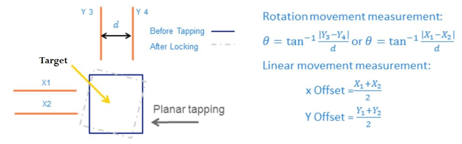
Tapping involves two major system functions – providing an input displacement system and measuring that the effect of the system provided the required results. Given ASML's need for precision alignment, measurements must include ensuring the desired displacement occurred without any undesired effects, such as rotational misalignment, as shown in Figure 4.
|
Figure 4: Tapping Displacements |
For your project, ASML will be looking to develop a "Super Tapper" consisting of an electromechanical tapping device capable of providing easily controllable displacements and having on-board position measurement capability. The device is intended for positioning bearing -slipper–locked mechanisms, which are dominated by stick-slip friction.
This effort will include the following requirements:
- Study the behavior of a simple bearing-slipper by manual tapping
- Research into current literature on tapping devices and related sensors, keeping in mind ASML's system requirements (clean room environment, etc.)
- System specs will be provided to students at the project kick-off meeting
- Propose solutions for controlled displacements and accurate metrology in the ~1 micron accuracy / precision range for ~ 1-3 mm of planar linear travel for sensitive targets, which would include optical modules
- Design control loop / feedback systems for the complete mechatronic device
- Self-calibration of electrical energy to displacement, adaptive to moderate variations in bearing slipper set up (bolt tension variations)
- Improved accuracy (~100 nm) would be a "stretch goal"
- Analyze the down-selected design choice for effects such as shock, stress, etc.
- Develop a test system to verify analytical assumptions and design choices
- Modify the analytical approach / final design if needed given test results
- Deliver "proof of concept" hardware of your system
End Game
In the end, if all goes as planned, you will have a quantifiable impact in helping ASML and its endeavors to keep Moore's Law alive for the next generation. You will have demonstrated knowledge of design and analysis, a key skill set in today's competitive job market. In addition, you will be an expert in making and measuring incredibly small adjustments by very simple (but smart) means.
This is by no means an easy endeavor, but we believe your group is up to it and you have 9 months to show us what you got.
If you have any questions, please contact:
Andy Judge
ASML Group Lead – Mechanical Development
andy.judge@asml.com
1 203 761 4328
Santiago Delpuero
ASML Senior Architect
santiago.delpuerto@asml.com
1 914 204 6245
Vasishta Ganguly
ASML Design Engineer
vasishta.ganguly@asml.com
1 203 761 4251
While they will help you, they will not do everything for you. Good luck (and skill)!
Cornell Project contact: Matt Ulinski (mu25@cornell.edu)